Why 172nm Excimer Technology Matters in the Next Generation of Semiconductor Manufacturing?
Aug 14, 2026
The artificial intelligence boom is changing more than the way we use technology. Behind every AI model, data center, and intelligent device is a rapidly evolving semiconductor industry that is investing heavily in more advanced chips, higher production capacity, and increasingly precise manufacturing processes.
As AI-driven demand continues to push semiconductor development forward, manufacturers are paying greater attention to every stage of the production process. Advanced chips require not only sophisticated equipment and materials, but also extremely clean and precisely controlled manufacturing environments. One often-overlooked challenge is organic contamination.
Even tiny amounts of organic residue can affect surface properties and process consistency during semiconductor manufacturing. This is one reason why advanced cleaning and surface-treatment technologies are attracting increasing attention.
Among these technologies, 172nm Excimer Lamp solutions offer an interesting approach through high-energy vacuum ultraviolet (VUV) radiation.
Why Does 172nm Light Matter?
A 172nm excimer lamp produces high-energy vacuum ultraviolet radiation that can interact strongly with organic molecules. The energy at this wavelength can break molecular bonds and promote photochemical reactions, making it useful for removing organic contaminants and modifying material surfaces.
Compared with conventional cleaning methods that may depend heavily on chemicals or physical contact, 172nm VUV technology provides a non-contact approach to precision surface treatment.
This makes it attractive for applications where cleanliness, process stability, precision, and equipment integration are important. For semiconductor manufacturing, potential applications include wafer surface cleaning, mask cleaning, organic contamination removal, and surface activation.
From AI Chips to Ultra-Clean Manufacturing
The global AI boom has created enormous demand for advanced semiconductors. However, producing these high-performance chips involves thousands of carefully controlled manufacturing steps. While people often focus on GPU performance, advanced process nodes, high-bandwidth memory, and packaging technologies, the cleanliness of semiconductor surfaces is equally important.
A small amount of organic contamination may appear insignificant, but at the microscopic level, it can interfere with subsequent processing steps. This is why semiconductor manufacturers are constantly exploring more efficient and precise cleaning technologies.
At www.gmyok.com, GMY provides UV and VUV light-source solutions for semiconductor, industrial, environmental, and other precision applications, including 172nm excimer products designed for different cleaning and surface-treatment requirements.
A Practical Solution for Cold Plate Organic Contamination
Semiconductor manufacturing is not the only area where organic contamination matters. Cold plates are increasingly important in high-performance electronics because efficient thermal management is essential for powerful computing systems, AI servers, and other high-density electronic equipment. As computing power continues to increase, manufacturers are looking for better ways to manage heat while maintaining high cleanliness standards.
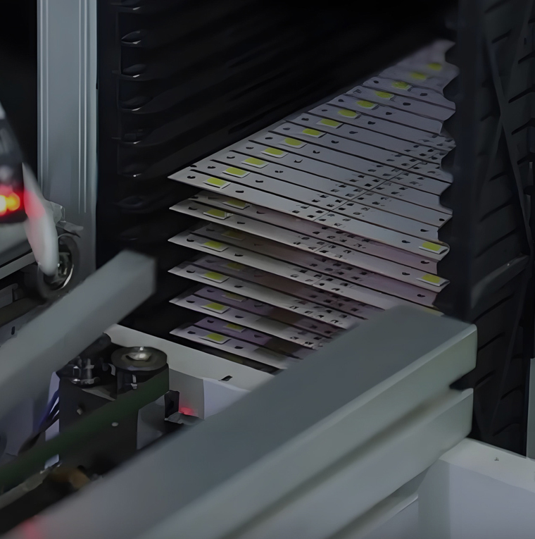
GMY's 172nm excimer module for cold plate organic particle applications provides a VUV-based solution for addressing organic contamination associated with cold plate processing. The modular design can be integrated into customized equipment and processing systems, giving equipment manufacturers greater flexibility when developing their own cleaning solutions.
For companies working on advanced thermal-management components, 172nm VUV technology provides another option for improving surface cleanliness without relying solely on traditional cleaning processes.
When Smaller Equipment Needs a Smaller Light Source
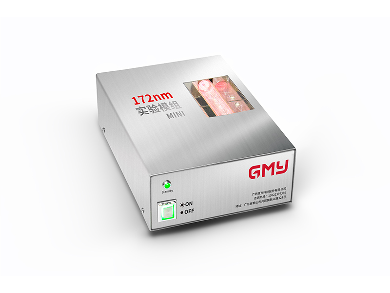
Not every semiconductor application requires a large production system. Research laboratories, universities, equipment manufacturers, and process-development teams often need compact light sources for testing, prototyping, and small-scale semiconductor processing. This is where GMY's 172nm mini excimer lamp module for Semiconductor Processing can provide a practical solution.
The compact module is designed for semiconductor-related processing applications where installation space and equipment integration are important considerations. It can provide high-energy VUV radiation for organic contamination removal and surface modification while maintaining a compact form factor. For engineers developing new semiconductor processing equipment, a mini excimer module can also make it easier to test VUV technology before moving toward a larger production system.
Beyond Semiconductor Cleaning
The potential applications of 172nm VUV technology extend beyond semiconductor processing. Because of its strong photochemical properties, 172nm excimer technology can also be explored for:
Organic contamination removal
Surface activation and modification
Ultrapure water TOC reduction
Optical component cleaning
Display substrate cleaning
Semiconductor mask cleaning
Industrial surface treatment
Photochemical oxidation
Water purification
One particularly interesting application is ultrapure water treatment. Semiconductor manufacturing requires extremely high-quality water, and controlling total organic carbon (TOC) is an important part of maintaining water purity. High-energy VUV radiation can promote photochemical oxidation reactions that help break down organic compounds. This makes 172nm excimer technology relevant not only to semiconductor surface processing but also to high-purity water applications.
Why Modular VUV Technology Matters
Modern industrial equipment is becoming increasingly customized. Different applications may require different irradiation areas, optical configurations, power levels, installation dimensions, and operating conditions. A standard light source may therefore not always be the most suitable solution. Modular excimer technology offers greater flexibility.
Instead of redesigning an entire system around a fixed lamp, manufacturers can integrate an appropriate VUV module into their existing equipment architecture. This is particularly useful for OEMs and equipment manufacturers developing specialized semiconductor cleaning, surface-treatment, cold plate processing, or water purification systems. At www.gmyok.com, customers can explore GMY's range of UV and VUV light-source products and contact the team to discuss customized requirements and OEM/ODM solutions.
The Future of Semiconductor Manufacturing Is in the Details
The next generation of semiconductor manufacturing will not be defined only by smaller process nodes and more powerful AI chips. It will also depend on countless details: cleaner surfaces, tighter process control, better materials, efficient equipment, and innovative manufacturing technologies. That is why 172nm excimer technology deserves greater attention.
Whether you are developing semiconductor cleaning equipment, researching surface modification, improving cold plate cleanliness, or exploring VUV applications for water purification, the right excimer light source can become an important part of your process.
GMY is committed to providing reliable UV and VUV light-source solutions for semiconductor processing, industrial applications, environmental technologies, and other precision applications. Want to learn more about 172nm excimer technology? Visit www.gmyok.com to explore GMY's 172nm excimer lamp and module solutions, or contact the GMY team to discuss your specific application and customization requirements.